How many Impedance of Pogo Pins?

Pogo pins, also known as spring-loaded connectors, are widely used in various electronic applications such as testing, prototyping, and interfacing between different electrical components. Given their crucial role in ensuring reliable electrical connections, understanding the impedance characteristics of pogo pin is essential for designers and engineers to optimize their performance. Impedance is an important electrical property that plays a role in signal integrity, power dissipation, and overall connector performance, especially in high-frequency and high-speed applications.
In this article, we will discuss what impedance means for pogo pins, the factors that influence it, typical impedance values, and how to mitigate impedance issues in designs that rely on pogo pins.
1. What is Impedance
Impedance is a complex measure of the opposition that a circuit presents to an alternating current (AC) signal. Unlike simple resistance, which applies to direct current (DC), impedance applies to AC signals and includes both resistance (R) and reactance (X) components, which can either be capacitive or inductive.
Resistance (R) The real part of impedance, which opposes the flow of current.
Reactance (X) The imaginary part of impedance, which opposes the flow of current due to capacitance or inductance. It varies with frequency.
For a pogo pin, impedance is a combination of its electrical resistance and the inductance or capacitance effects due to its physical properties (such as size, materials, and geometry).
2. Impedance in Pogo Pins
In typical applications, the impedance of a pogo pin can be thought of as the opposition it offers to an AC signal at a given frequency. Since pogo pins are primarily used in low- to medium-frequency applications (like testing, signal connections, and data transfer), their impedance characteristics are influenced by
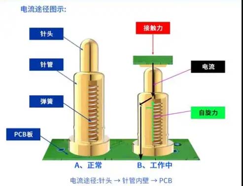
Contact Resistance The resistance at the point of contact between the pogo pin and the pad or PCB. This resistance depends on factors like material, plating, and contact pressure.
Inductive Effects The shape and size of the pogo pin and the associated spring can induce inductance. The geometry of the pin itself, such as its length and diameter, affects how it behaves as an inductive element.
Capacitive Effects The gap between the pogo pin and the pad, as well as the dielectric material surrounding the pin, creates a capacitor. This capacitance is frequency-dependent and influences the impedance at high frequencies.
For most general-purpose applications, the impedance of a pogo pin is not usually a critical design consideration. However, in high-speed data transmission, high-frequency circuits, and certain power applications, understanding and controlling impedance becomes important to ensure signal integrity and efficient power delivery.
3. Factors Influencing the Impedance of Pogo Pins
Several factors influence the impedance of a pogo pin, and these factors must be considered when designing for high-performance applications.
3.1 Contact Resistance
The most immediate and noticeable contribution to the impedance of a pogo pin is the contact resistance. This is the resistance encountered when the pogo pin makes contact with the target pad or PCB. Contact resistance is influenced by
Material of the Pin Materials with higher conductivity, like gold or silver, have lower contact resistance. For example, gold is often used for high-reliability applications because it resists oxidation, ensuring a stable connection over time.
Contact Pressure The spring mechanism inside the pogo pin applies pressure to ensure good contact. If the pressure is too low, the contact area could be too small, resulting in high resistance and poor signal transmission. On the other hand, excessive pressure can cause wear on the contacts.
Surface Condition Any contaminants or oxidation on the surface of the pogo pin or the pad can increase contact resistance, leading to higher impedance and potential signal loss.
The contact resistance for a typical pogo pin is usually in the range of milliohms (mΩ), typically between 1 mΩ and 20 mΩ, depending on the quality of the connection and materials used.
3.2 Inductive Effects
Inductance arises due to the physical structure of the pogo pin and its internal spring mechanism. When alternating current flows through the pin, the changing magnetic fields generated by the current induce inductive opposition to the flow of current. The amount of inductance depends on
Pin Length A longer pin creates more inductance because it has a greater length for the current to travel through.
Diameter of the Pin A larger diameter pin has a smaller resistance to current flow but can also induce higher inductance.
Spring Mechanism The internal spring, which maintains contact pressure, also has inductive properties. The type of spring material and its geometry can affect the overall inductance of the pin.
In most cases, the inductance of a pogo pin is relatively small but becomes more significant at higher frequencies. Typical values for inductance in pogo pins can range from 10 nH to 100 nH, though they can be higher depending on the design.
3.3 Capacitive Effects
Pogo pins can also behave as capacitors due to the dielectric gap between the pin’s contact tip and the target pad. This capacitance arises from
Gap Distance The physical distance between the contact tip and the PCB or pad is a key factor in determining the capacitance. A smaller gap increases the capacitance, whereas a larger gap reduces it.
Dielectric Material The material surrounding the pogo pin also affects the capacitance. Air has a dielectric constant of approximately 1, while materials like plastics or ceramics can have higher dielectric constants, increasing the capacitance.
Pin Size and Shape The geometry of the pogo pin, including the surface area of the contact tip, affects how much capacitance is created. Larger contact areas generally result in higher capacitance.
Capacitance becomes more significant at higher frequencies. In high-speed data transfer applications or signal integrity-sensitive environments, the capacitance of the pogo pin may need to be carefully managed to prevent signal distortion or interference.
Typical capacitance values for a pogo pin can range from 0.1 pF to several pF, depending on the design. This capacitance becomes more critical when dealing with high-frequency signals or when the pogo pins are used in high-speed digital circuits.
3.4 Frequency Dependence
The impedance of a pogo pin is frequency-dependent. At low frequencies, the resistance tends to dominate, but as the frequency increases, both inductive and capacitive effects start to play a more significant role. In high-frequency applications, the inductance and capacitance of the pogo pin can cause signal attenuation, phase shifting, and potential signal integrity issues.
In signal transmission lines, particularly for high-speed digital signals, managing the impedance of connectors (including pogo pins) is essential to maintain signal quality. For these applications, it is crucial to maintain a controlled characteristic impedance, typically around 50 Ω or 75 Ω, to match the impedance of the transmission line and avoid signal reflections.
4. Typical Impedance Values for Pogo Pins
The impedance of a pogo pin is not typically specified for most low-frequency or low-speed applications. However, it can be characterized in terms of its contact resistance, inductive reactance, and capacitive reactance
Contact Resistance Generally in the range of 1 mΩ to 20 mΩ for a well-designed pogo pin.
Inductive Reactance Typically ranges from 10 nH to 100 nH, depending on the design.
Capacitive Reactance Usually between 0.1 pF to several pF.
For high-speed or high-frequency applications, the combined impedance can range from 50 Ω to 100 Ω or higher, depending on the size, design, and material choices. The actual impedance for these specialized high-speed applications needs to be carefully matched with the surrounding circuitry to ensure that signal integrity is maintained.
5. Reducing Impedance Issues in Pogo Pin Designs
In high-speed or high-frequency designs, managing impedance is critical to ensure proper signal transmission and prevent issues like signal reflections, loss, or distortion. Some strategies for managing impedance in
pogo pin designs include
1. Optimizing Contact Area and Pressure Ensuring proper contact pressure and maximizing the contact area can reduce contact resistance, which in turn reduces impedance.
2. Using High-Quality Materials Gold or silver plating on contact points reduces resistance and provides better signal transmission, especially for high-frequency signals.
3. Reducing Inductive Effects Minimizing the length of the pogo pin, selecting appropriate spring designs, and ensuring proper pin orientation can reduce inductive reactance.
4. Minimizing Capacitance Reducing the gap between the pin and the target pad, using materials with lower dielectric constants, and limiting the surface area of the pin can help minimize capacitance effects in high-frequency designs.
5. Impedance Matching In high-speed applications, it's crucial to match the impedance of the pogo pin to that of the surrounding circuits or transmission lines to prevent signal reflection or loss.
The impedance of pogo pins is a combination of contact resistance, inductive reactance, and capacitive reactance, all of which can affect the performance of the connector in various applications. For low-frequency and low-speed applications, the impedance of a pogo pin is typically not a major concern. However, for high-speed or high-frequency circuits, impedance can have a significant impact on signal integrity. Understanding the factors that influence pogo pin impedance and selecting the right pin design for your specific application is crucial to maintaining reliable performance
